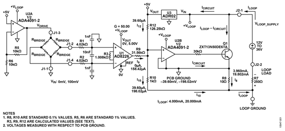
The design provides a complete solution for the 4 mA-to-20 mA transmitter for #pressure sensor measurements where the supply for the entire circuit is provided by the loop. The circuit has three critical stages: the sensor excitation drive, sensor output amplifier, and the voltage to current converter.
The total current required by the circuit is 1.82 mA (maximum) as shown in Table 1. Pressure sensors requiring bridge drive currents of up to 2 mA can therefore be used without exceeding the maximum available loop current of 4 mA.

Table
The .table-bordered class adds border on all sides of the table and cells:
Circuit Function & Benefits
The circuit shown in Figure 1 is a robust and flexible loop-powered current transmitter that converts the differential voltage output from a pressure sensor to a 4 mA-to-20 mA current output.
The design is optimized for a wide variety of bridge based voltage or current driven pressure sensors, utilizes only four active devices, and has a total unadjusted error of less than 1%. The loop supply voltage can range from 12 V to 36 V.
The input of the circuit is protected for ESD and voltages beyond the supply rail, making it ideal for industrial applications.


Circuit Description
The design provides a complete solution for the 4 mA-to-20 mA transmitter for pressure sensor measurements where the supply for the entire circuit is provided by the loop. The circuit has three critical stages: the sensor excitation drive, sensor output amplifier, and the voltage to current converter.
The total current required by the circuit is 1.82 mA (maximum) as shown in Table 1. Pressure sensors requiring bridge drive currents of up to 2 mA can therefore be used without exceeding the maximum available loop current of 4 mA.
| Component |
Current(mA) |
| ADR02 |
0.80 |
| ADA4091-2 |
0.50 |
| AD8226 |
0.43 |
| R5, R6 @ 10V |
0.05 |
| R12 @ 5V |
0.04 |
| TOTAL |
1.82 |
Sensor Excitation Drive
Depending on the pressure sensor selected, either a voltage or current drive is required. The circuit uses one half of the ADA4091-2 (U2A) with different configurations chosen by switching S1 to support either option. The switch S1 provides the selection for either drive.
Excitation: Voltage Drive Configuration
Figure 2 shows the configuration for the voltage drive with S1 in the position labeled VOLTAGE DRIVE on the PCB (see complete circuit layout and schematics in the CN0289 design support package: http://www.analog.com/CN0289-DesignSupport).


The voltage drive circuit is normally configured for a bridge drive voltage of 10 V. In this mode, the minimum allowable bridge resistance is:

For lower than 5 kΩ bridge resistance, the drive voltage can be decreased down to 5 V using a buffer configuration by removing R6.
Other values of drive voltage can be obtained by properly selecting R6 using the equation:

where

Note that the loop voltage, VLOOP, should be at least 0.2 V greater than the bridge drive voltage to allow sufficient headroom for U2A.

Excitation: Current Drive Configuration
The circuit can be switched to the current drive configuration shown in Figure 3 by moving S1 to the position labeled CURRENT DRIVE on the PCB.


In the current drive mode, the 2 mA maximum allowable bridge drive current must be observed. The circuit is configured for R4 = 2.49 kΩ, and IDRIVE = 2 mA. Lower values of IDRIVE can be obtained by using the following equation to select the value of R4:

The resulting drive voltage VDRIVE is calculated from:

A headroom of 0.2 V is required for the U2A supply, therefore:

For the values shown in Figure 3, RBRIDGE = 3 kΩ, IDRIVE = 2 mA, VDRIVE = 11 V, and VLOOP ≥ 11.2 V.
The ADA4091-2 op amp is chosen for the circuit because of its low current consumption (250 μA/amplifier), low offset voltage (250 μV), and rail-to-rail inputs and outputs.
Bridge Output Instrumentation Amplifier and Selection of Gain and Offset Resistors
The output of the bridge is filtered by a common-mode filter (4.02 kΩ, 1 nF) with a bandwidth of 39.6 kHz and a differential-mode filter (8.04 kΩ, 10 nF) with a bandwidth of 2 kHz.
The AD8226 is an ideal choice for the in-amp because of its low gain error (0.1%, B-grade), low offset (58 μV @ G = 50, B-grade; 112 μV @ G = 50, A-grade), excellent gain nonlinearity (75 ppm = 0.0075%), and rail-to-rail output.
The AD8226 instrumentation amplifier amplifies the 100 mV FS signal by a factor of 50 V to 5 V using a gain setting resistor R3 = 1.008 kΩ. The relationship between the gain, G, and R3 is given by

where G = 50, and R3 = 1008 Ω.
For the output zero-value loop current, ILO = 4 mA:

Because of the 100:1 ratio of R10 to R8:

Combining the last two equations:

The AD8226 output is 0 V for ILO = 4 mA, and the offset resistor R12 can now be calculated from:

For VOUT= 5.00V, the output loop current is ILH = 20 mA, and hence:


The current through R12 is given by:

The current through R9 is given by:

The value of R9 can now be calculated from:

In practice, the calculated values for R3, R12, and R9 will not be available as standard values, so there will be fixed errors introduced by the actual values used in the circuit. These errors can be calculated as follows. Gain, offset, and total error, measured as a %FSR (where FSR = 16 mA) due to resistors R3, R9, and R12:

The total error at zero output (4 mA) is not affected by the gain error.
However, the total error at full-scale output (20 mA) is equal to:
Full Scale Error = Gain Error + Offset Error
In the practical circuit, the nearest EIA standard 0.1% resistor values must be chosen, thereby resulting in fixed gain and offset errors as described in the previous equations. It is possible to use combinations of two 0.1% values to come closer to the calculated values. For instance, the following series combinations of 0.1% resistors come very close to the calculated values:
- R3 = 1 kΩ + 8.06 Ω = 1008.06 Ω (calculated = 1008 Ω)
- R9 = 30.9 kΩ + 655 Ω = 31.555k Ω (calculated = 31.56 kΩ)
- R12 = 124 kΩ + 2.26 kΩ = 126.26 Ω (calculated = 126.25 Ω)
The error calculated with these combinations is as follows:
- Offset Error = −0.008% FSR
- Gain Error = +0.010% FSR
- Full Scale Error = +0.002% FSR
In some cases, however, even standard 0.1% resistor values may not be obtainable from resistor suppliers, and substitutions are required.
For example, the resistors supplied with the EVAL-CN0289-EB1Z board are as follows:
- R3 = 1000 Ω (calculated = 1008 Ω)
- R9 = 31.6 kΩ (calculated = 31.56 kΩ)
- R12 = 124 kΩ (calculated = 126.25 kΩ)
With the values supplied with the board, the errors due to the resistor values are:
- Offset Error = +0.45% FSR
- Gain Error = +0.66% FSR
- Full Scale Error = +1.11% FSR
Voltage Reference
The ADR02 5 V reference is used to set the drive voltage or current to the bridge and to set the 4 mA zero offset. It has an initial accuracy of 0.1% (A-grade), 0.06% (B-grade), and 10 μV p-p voltage noise. In addition it will operate on supply voltages up to 36 V and consumes less 1 mA maximum, making it an ideal choice for loop-powered applications.
The 4 mA-to-20 mA output is produced by forcing a current through R10 that is the sum of the signal component (I9) and the offset component (I12). The current I10 = I9 + I12 develops a voltage across R10 that is applied to the sense resistor R10 through U2B and Q1. The current through R8 is 100× the current in R10. The loop current, ILOOP, is therefore :

The values of R8 (10 Ω) and R10 (1 kΩ) were chosen to be values that are easily obtainable in 0.1% tolerances.
In order for the circuit to operate properly, the circuit current, ICIRCUIT, must always be less than the minimum loop current of 4 mA. In addition, the ground of the PCB must not be connected to the loop ground in any manner, and the PCB ground and the sensor must be free to float with respect to the loop ground.
The bipolar NPN transistor that is controlled by the output of U2B and generates the loop current should have a gain of at least 300 to minimize the linearity error. It should also have a breakdown voltage of at least 50 V.
The output transistor Q1 is a 50 V NPN power transistor capable of dissipating 1.1 W @ 25°C. The worst case power dissipation in the circuit is for an output current of 20 mA into a loop load resistance of 0 Ω with a VCC supply of 36 V. Under these conditions the power dissipation of Q1 is 0.68 W.
The supply voltage, VLOOP, driving the circuit board is dependent on the loop supply VLOOP_SUPPLY, the loop load, R7, and the loop current, ILOOP. These values are related by the following equation:

In order for the circuit to operate properly, the supply voltage, VLOOP, must be greater than 7 V in order to provide sufficient headroom for the ADR02 voltage reference.
Therefore,

For a maximum loop current of 20 mA, and R7 = 250 Ω,

The minimum loop supply voltage is also dependent on the configuration of the drive circuit for the bridge. In the voltage drive mode with VDRIVE = 10 V, the supply voltage VLOOP must be greater than 10.2 V in order to maintain sufficient headroom for U2A (see Figure 2).
In the current drive mode, the supply voltage VLOOP must be greater than 11.2 V in order to maintain sufficient headroom for U2A (see Figure 3).
The loop supply voltage is limited to 36 V maximum.
Error Analysis for Active Components
The maximum and rss errors due to the active components in the system for A- and B-grade levels of the AD8226 and ADR02 are shown in Table 2 and Table 3. Note that the ADA4091-2 op amp is only available in one grade level.
| Error Component | Error | Error Value | Error %FSR |
| AD8226-A ADR02-A ADA4091-2 AD8226-A |
Offset Offset Offset Gain |
112µV 0.10% 250µV 0.15% |
0.11% 0.02% 0.16% 0.15% |
| RSS Offset RSS Gain RSS FS Error |
0.20% 0.15% 0.35% |
||
| Max Offset Max Gain Max FS Error |
0.29% 0.15% 0.44% |
| Error Component | Error | Error Value | Error %FSR |
| AD8226-B ADR02-B Offset ADA4091-2 Offset AD8226-B Gain |
Offset Offset Offset Gain |
58µV 0.06% 250µV 0.10% |
0.06% 0.01% 0.16% 0.10% |
| RSS Gain RSS Offset RSS FS Error |
0.10% 0.17% 0.27% |
||
| Max Offset Max Gain Max FS Error |
0.23% 0.10% 0.33% |
Total Circuit Accuracy
A good approximation to the total error contributed by the resistor tolerances is to assume that each of the critical resistors contribute equally to the total error. The five critical resistors are R3, R8, R9, R10, and R12. Worst-case tolerance build up of 0.1% resistors yields a total resistor error of 0.5% maximum. If rss errors are assumed, then the total rss error is 0.1√5 = 0.224%.
- Offset Error = 0.29% +0.5% = 0.79%
- Gain Error = 0.15% + 0.5% = 0.65%
- Full Scale Error = 0.44% + 0.5% = 0.94%
These errors assume ideal resistors are selected and that the only errors are due to their tolerances.
Although the circuit is capable of 1% or less total error, if better accuracy is required offset and gain adjustment capability should be added to the circuit. Offset can be calibrated by adjusting R12 for 4 mA output with zero input, and full-scale can then be adjusted by varying R9 for a full-scale 100 mV input. The two adjustments are independent provided the offset is calibrated first.
Actual error data from the circuit is shown in Figure 4. The total output error (%FSR) is calculated by taking the difference between the ideal output current and the measured output current, dividing by the FSR (16 mA), and multiplying the result by 100.
Note that the error between 0 mV and 1 mV input is due to the saturation voltage of the AD8226 output stage that can range from 20 mV to 100 mV under the loading conditions in the circuit. All rail-to-rail output stages are limited in their ability to approach the supply rails by either the saturation voltage (bipolar outputs) or on-resistance (CMOS outputs).
If the error caused by the output saturation voltage is troublesome, the input signal from the bridge can be offset by connecting an appropriate resistor from the +5 V reference to one side of the bridge output.


Common Variations
The circuit is proven to work with good stability and accuracy with component values shown. Other voltage references, precision op-amps and in-amp can be used in this configuration to develop 4 mA-to-20 mA analog current output and for other various applications for this circuit.
The ADA4091-4 is a quad version and can be used as a substitute for the ADA4091-2, dual channel, if additional precision op amps are needed.
The AD8426, a dual-channel, low cost, and wide supply range instrumentation amplifier can also be used for multiple input channel applications.
The ADR4550, high precision, low power, low noise voltage references can be used to replace ADR02 for a low voltage supply applications.
Circuit Evaluation & Test
Equipment Required
- EVAL-CN0289-EB1Z evaluation board
- Agilent E36311A dual dc power supply or equivalent
- Agilent 3458A multimeter or equivalent
Current Output Measurement
The current output of the evaluation board was measured with a setup seen in Figure 5. The test conditions were as follows:
- Loop supply: 24 V
- Loop load: 250 Ω
- RBRIDGE = 3 kΩ
- VDRIVE = 5 V
- VCM = 2.5 V
The bridge resistors are connected to both terminal inputs of the in-amp to simulate sensor output.
Test Setup Configuration and Tests
The circuit was tested using the test setup in Figure 5.
The Agilent E36311A dual power supply was used to generate a common-mode voltage of 2.5 V and a 0 mV to 100 mV differential input voltage.
The Agilent 3458A was used to measure the actual loop current output of the evaluation board.


Comments
Post a Comment